Review: nVidia GeForce GTX 660 & SLI
Published by Christian Ney on 13.09.12Technical data / specifications
With the nVidia GeForce GTX 660 you get a graphics card priced just under the 190 Euros range (without VAT) that should be fast enough to provide best gaming experience. The manufacturer claims that the fresh new GTX 660 is up to 60 % faster than Fermi's GTX 460 and 16 % faster than AMD's HD 7850.
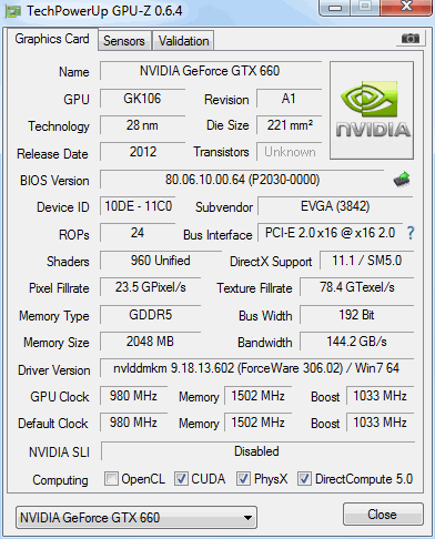
Looking at clock speeds we see that the GPU runs at 980 MHz standard with a
typical boost clock of 1'033 MHz. For the record the Boost Clock speed is based on the average GeForce GTX 660 card running a wide variety of games and applications. Note that the actual Boost clock will vary from game-to-game depending on actual system conditions
with a 13 MHz step.
The memory subsystem of the GeForce GTX 660 consists of three 64-bit memory
controllers (192-bit) with 2GB of GDDR5 memory clocked at 1'502 MHz (rated 6'008
MHz, americans like big numbers you know). While the memory clock speed and
memory technology/amount stay the same as with the GK104 based
graphics cards, the memory interface is different. Instead of a 256 Bit
interface (GTX
680/670) you'll find a 192 Bit interface (GTX 660 Ti/660). This also reduces the
available memory bandwidth from
192'400 MB/s to 144'000 MB/s.
The GK106 GPU itself consists of 2.54 billion transistors, 1 billion less
than the GK104. Then you find 960 CUDA cores aka 5 SMX units, 80 texture units
and 24 ROPs. We compared it to the GTX 670 and GTX 660 Ti in the table below.
About the power consumption, here is what nVidia says:
Under load, the GeForce GTX 660 typically draws up to 115W of power in most non-TDP apps. This is what you�ll experience with the power target slider set at its default 100% setting. If you wish to overclock the GeForce GTX 660, we highly recommend that you max the slider out at +110%. At this setting, the board will draw up to 127W in non-TDP
apps.
| GeForce GTX 670 | GeForce GTX 660 Ti | GeForce GTX 660 | |
| Chip | GK104 | GK104 | GK106 |
| Process | 28 nm | 28 nm | 28 nm |
| Transistors | 3.54 billion | 3.54 billion | 2.54 billion |
| GPU clock | 915 MHz (Boost 980 MHz) | 915 MHz (Boost 980 MHz) | 980 MHz (Boost 1'033 MHz) |
| Memory | 2'048 MB GDDR5 | 2'048 MB GDDR5 | 2'048 MB GDDR5 |
| Memory clock | 6'000 MHz | 6'000 MHz | 6'000 MHz |
| Memory interface | 256 Bit | 192 Bit | 192 Bit |
| Memory bandwidth | 192'400 MB/s | 144'000 MB/s | 144'000 MB/s |
| TMUs | 112 | 112 | 80 |
| TAUs | -- | -- | -- |
| Shader Cores | 1'344 (5D) | 1'344 (5D) | 960 (5D) |
| ROPs | 32 ROP | 24 ROP | 24 ROP |
| Shader model | SM 5 | SM 5 | SM 5 |
| Maximum board power | 170 Watt | 150 Watt | 140 Watt |
Discuss this article in the forums


| Navigate through the articles | |
 Review: ASUS GeForce GTX 660 Ti DirectCU II Top
 |
Review: EVGA GeForce GTX 650 Ti 2GB SSC SuperSuperClocked
 |
|
|