Review: EVGA GTX 680 Superclocked
Published by Marc Büchel on 25.07.12Technical data / specifications
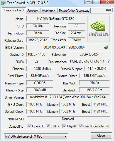
With the EVGA GTX 680 Superclocked you get a factory overclocked card, which is based on NVIDIAs latest GK-104 chip, that is being manufactured at TSMC using 28 nanometer structures. Most factory overclocked card feature either a modified cooler, a modified PCB or both. With the GTX 680 Superclocked EVGA chose to modify neither of these things. The card comes with the NVIDIA reference design and cooler.Looking at cock speeds we see that the GPU runs at 1'058 MHz standard and 1'124 MHz boost clock. The GDDR5 memory clocks at 6'208 MHz. Furhtermore there is 256 bit memory interface which results in 198'656 Megabyte per second memory bandwidth. In total there is 2'048 Megabyte of GDDR5 memory.
The GPU itself consists of 3.54 billion transistors. The architectural hierarchy starts with a so called GigaThread Engine, which marshals processed and unprocessd information between the GPU and the PCI-Express 3.0 system interface. Further down in the hierarchy there are four Graphics Processing Clusters (GPCs), which can be seen as a common resource. At this point you'll also find a the raster eingine and two streaming multiprocessors (SMs). Altough NVIDIA decided to change their name which means that they're now called SMX.
| GeFroce GTX 680 | EVGA GTX 680 SuperClocked | Radeon HD 7970 | Radeon HD 7950 | |
| Chip | GK104 | GK104 | Tahiti | Tahiti |
| Process | 28 nm | 28 nm | 28 nm | 28 nm |
| Transistors | 3.54 billion | 3.54 billion | 4.31 billion | 4.31 billion |
| GPU clock | 1'006 MHz (Boost 1'058 MHz) | 1'058 MHz (Boost 1'124 MHz) | 925 MHz | 800 MHz |
| Shader clock | 1'006 MHz | 1'058 MHz | 925 MHz | 800 MHz |
| Memory | 2'048 MB GDDR5 | 2'048 MB GDDR5 | 3'072 MB GDDR5 | 3'072 MB GDDR5 |
| Memory clock | 6'000 MHz | 6'208 MHz | 5'500 MHz | 5'000 MHz |
| Memory interface | 256 Bit | 256 Bit | 384 Bit | 384 Bit |
| Memory bandwidth | 192'400 MB/s | 198'656B/s | 264'000 MB/s | 240'000 MB/s |
| TMUs | 128 | 128 | 128 | 2x 96 |
| TAUs | -- | -- | 128 | 2x 96 |
| Shader Cores | 1'536 (5D) | 1'536 (5D) | 2'048 (1D) | 1'792 (1D) |
| ROPs | 32 ROP | 32 ROP | 32 ROP | 32 ROP |
| Shader model | SM 5 | SM 5 | SM 5.1 | SM 5.1 |
| Maximum board power | 185 Watt | >185 Watt | 250 Watt | 200 Watt |
Discuss this article in the forums


| Navigate through the articles | |
 Preview: nVidia GK110 Performance Analysis
 |
Review: ASUS GeForce GTX 660 Ti DirectCU II Top
 |
|
|